
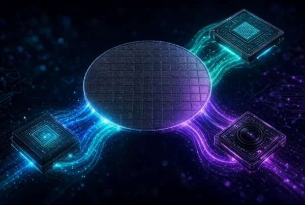
The Silent Grid Emergency
The cooling fans inside a hyperscale data center spool up to maximum velocity, producing a mechanical whine that vibrates through steel server racks. It is 2:14 AM. An incoming wave of tens of millions of multimodal requests strikes the network interface cards simultaneously.
Every millisecond of latency threatens catastrophic timeouts across automated financial ledgers, edge sensor fleets, and consumer platforms. As the orchestration layer routes the incoming queries, standard central processors quickly cross thermal throttles. Megawatts spike across power distribution units. Copper buses heat up. Despite row after row of high-frequency general-purpose silicon, the compute queue chokes.
The machine is trying to calculate a marathon using a Swiss Army knife.
Then, the cluster scheduler diverts the heaviest matrix math tasks to dedicated silicon. Temperatures stabilize. Latency collapses from hundreds of milliseconds to single digits. The grid survives another surge.
This tension defines the modern hardware landscape. As workloads multiply exponentially, general-purpose processors can no longer satisfy demand on their own. Enter Application-specific semiconductors, the specialized silicon architectures rescuing compute and connectivity from a looming physical wall.
Why are specialized chips becoming essential when flexible processors carried computing for over half a century?
Table of Contents Of Application-Specific Semiconductors
What Are Application-Specific Semiconductors?
To understand this architectural pivot, consider how silicon operates.
A traditional central processing unit (CPU) is built as a brilliant generalist. It can balance an operating system, execute complex branching logic, browse the web, and run spreadsheets. To deliver that versatility, a large percentage of its physical silicon area accommodates instruction decoders, branch prediction logic, and sprawling memory caches. Very little of the actual die area performs raw arithmetic calculations simultaneously.
Application-specific semiconductors, frequently implemented as Application-Specific Integrated Circuits (ASICs), abandon generalist flexibility intentionally.
Engineers design an application-specific chip to execute one task or a narrow family of tasks with maximum physical efficiency. By stripping away extraneous execution units and instruction translation layers, the physical design reflects the underlying mathematical equations of the workload.
If an algorithm relies almost entirely on matrix multiplications, the chip features vast grids of multiply-accumulate units interconnected by dense, low-latency memory paths. Doing one thing exclusively eliminates instruction overhead, maximizes throughput per clock cycle, and dramatically reduces wasted electrical energy.
Why Application-Specific Semiconductors Are Changing
For decades, the semiconductor industry relied on Dennard scaling and traditional lithography shrink cycles to make general computing faster and cheaper without drawing significantly more power. That physical free lunch has largely concluded. Transistors can still shrink, as documented by foundry roadmaps at TSMC, but running them at higher clock frequencies creates unsustainable thermal bottlenecks.
At the same time, computing demands have undergone an unprecedented inflection point driven by:
- Large-scale generative AI and deep neural network training
- Real-time automated inference at the edge
- Exponential expansion of hyperscale cloud infrastructure
- Complex software-defined networking fabrics
- Sensor fusion across modern transportation platforms
One architecture cannot balance extreme speed, minimal latency, low unit cost, and energy limits across divergent software stacks. When an enterprise processes petabytes of neural network operations daily, running them on general-purpose chips wastes both electricity and board footprint.
Specialization matches the underlying physical physics of the silicon directly to the mathematical profile of the workload.
The Connectivity Frontier
Computing cannot be treated separately from connectivity. A state-of-the-art processor is useless if data remains trapped in routing queues or constrained by physical pin bandwidth.
Modern high-speed communications, spanning 5G deployments, 5G Advanced rollouts, and exploratory 6G research tracked by groups like the ITU, demand massive digital signal processing throughput within microsecond windows. Massive MIMO antenna systems must adjust phase, amplify signals, and decode hundreds of spatial channels in real time.
General-purpose silicon cannot handle this volume of analog-to-digital translation and signal separation within reasonable power constraints. Cellular base stations and edge radios lean entirely on specialized silicon:
- Digital front-end ASICs to synthesize high-bandwidth radio frequencies
- Dedicated network packet processors to route line-rate traffic across switches
- Edge inference chips designed to analyze camera streams locally without round-tripping data to remote clouds
As edge environments like smart factories and connected electric vehicles evolve, compute and connectivity merge into a single technological layer. A vehicle making an obstacle avoidance decision cannot tolerate long round-trip delays over cloud networks. The sensor processing, telemetry decompression, and neural network inference must happen locally, across dedicated, co-located chips.
Why Specialization Matters: The Engineering Advantages
When an engineering team builds a platform around Application-specific semiconductors, they gain critical technical benefits:
+-------------------------------------------------------------+
|                      Silicon Specialization                 |
+------------------------------+------------------------------+
| Higher Compute Density       | Strips unnecessary logic;    |
|                              | dedicates area to execution  |
+------------------------------+------------------------------+
| Minimized Latency            | Hardwires data paths; cuts   |
|                              | instruction decode cycles    |
+------------------------------+------------------------------+
| Deterministic Timing         | Eliminates variable OS       |
|                              | interrupts on execution pins |
+------------------------------+------------------------------+
| Superior Power Efficiency    | Reduces wasted joules per    |
|                              | useful mathematical task     |
+------------------------------+------------------------------+
- Energy Efficiency: Traditional chips burn significant energy simply managing instructions and fetching data back and forth through deep cache hierarchies. Dedicated silicon aligns physical memory closely with logic units, saving milliwatts on every operation.
- Ultra-Low Latency: In networking and financial trading, software layers add jitter. Hardwiring logic directly into the silicon allows signals to traverse input to output in nanoseconds.
- Hardware-Enforced Security: Purpose-built silicon can isolate cryptographic keys and critical execution pipelines at the physical layer, making side-channel eavesdropping and memory corruption attacks significantly harder to execute, aligning with benchmarks from NIST.
- Predictable Performance: General-purpose software environments suffer from noisy neighbors and unpredictable scheduling delays. Dedicated chips operate with mathematical determinism, an essential requirement for aerospace systems and industrial robotics.
Architectural Tradeoffs: General Purpose vs Specialized Silicon
| Characteristic | General-Purpose Processor (CPU) | Application-Specific Semiconductor (ASIC) | Field-Programmable Gate Array (FPGA) |
| Workload Flexibility | High (Runs any program) | Fixed (Executes intended task only) | Medium (Reconfigurable via software) |
| Development Cost | Low (Amortized over billions) | Extremely High (Tens of millions USD) | Medium (Higher chip cost, no tape-out) |
| Time to Market | Immediate (Off the shelf) | Slow (18 to 36 month design cycle) | Moderate (Weeks to months of coding) |
| Energy Efficiency | Baseline | Exceptional (10x to 100x advantage) | Moderate |
| Silicon Area Utilization | Generalist logic dominant | 100% dedicated to target function | Overhead for reconfigurable routing |
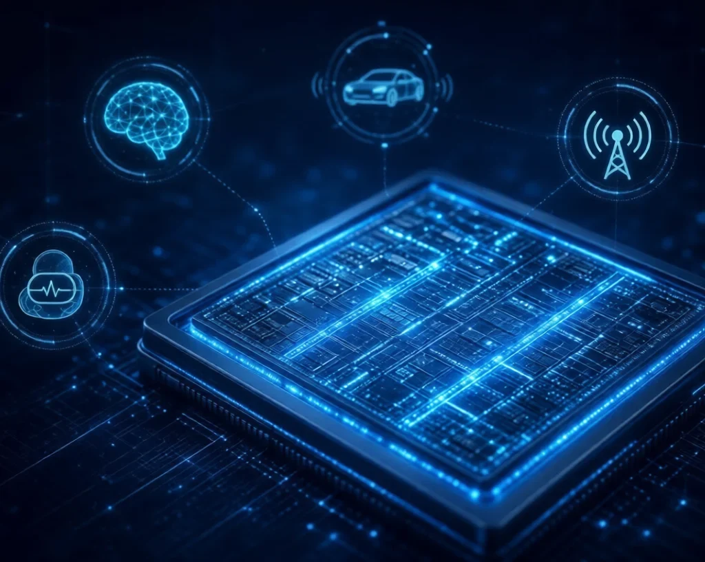
The Hidden Cost of Pure Specialization
Specialized hardware is not an automatic solution for every computing hurdle. Moving away from standard components introduces substantial financial and operational risks that organizations must evaluate.
Developing custom silicon carries high Non-Recurring Engineering (NRE) costs. Designing modern microchips requires specialized talent, multi-million-dollar electronic design automation (EDA) licenses, and verification testing. Mask sets at cutting-edge nodes cost millions before a single wafer is produced.
A project must operate at massive scale to amortize these front-loaded capital expenditures. If an organization manufactures only 10,000 units, the cost per chip can prove financially non-viable compared to buying commercially available processors.
There is also the constant risk of algorithmic obsolescence. Silicon design cycles often require two to three years from whitepaper architecture to packaged silicon. If the target artificial intelligence model or transmission standard changes while the chip is in development, the resulting silicon may arrive obsolete. In contrast, general-purpose hardware adapts simply by downloading a software patch.
Specialized silicon is also deeply dependent on a concentrated global supply chain, an issue tracked closely by the Semiconductor Industry Association. From advanced lithography tools to specialized packaging foundries, any disruption in raw materials, wafer production, or intellectual property licensing can halt an entire hardware rollout.
Mini Case Study: Google Cloud Tensor Processing Units (TPUs)
To see the economic and operational value of custom silicon in real infrastructure, consider Google’s development of the Tensor Processing Unit.
Incoming Deep Learning Requests
               │
               ▼
┌──────────────────────────────┐
│  Host CPU: Routes work,      │
│  coordinates networking      │
└──────────────┬───────────────┘
               │ PCI Express Bus
               ▼
┌──────────────────────────────┐
│  Custom TPU Silicon          │
│  ┌────────────────────────┐  │
│  │ Two-Dimensional Matrix │  │  Executes dense matrix math directly
│  │ Multiply Unit (Systolic│  │  with no instruction-fetch overhead
│  │ Array Architecture)    │  │
│  └────────────────────────┘  │
│  Integrated On-Chip Memory   │
└──────────────────────────────┘
- The Challenge: Around 2013, internal projections indicated that if voice search and deep neural networks were used by consumers for just several minutes a day, total data center compute capacity would need to double, requiring immense capital expenditure on general-purpose servers.
- The Workload: Neural network inference, heavily dominated by dense matrix multiplications and additions rather than complex conditional branching.
- The Silicon Approach: Google engineers created the TPU v1, a dedicated coprocessor connected via a PCIe slot. Instead of relying on traditional caches and complex instruction decoders, the chip uses a systolic array design. Data streams continuously through a two-dimensional grid of arithmetic units, multiplying and adding without reading and writing back to memory registers at each step.
- The Documented Outcome: In research published with the IEEE, the design delivered roughly 15 to 30 times higher performance per watt than contemporaneous general CPUs and GPUs on target inference workloads.
- The Broader Lesson: When a software workload becomes mathematically predictable and runs at massive scale, developing custom silicon stops being an expensive novelty; it becomes an operational necessity.
The Bigger Picture: Heterogeneous Computing and Co-Design
The computing ecosystem is not heading toward an absolute zero-sum conflict where dedicated chips replace general-purpose processors entirely. Instead, the frontier relies on heterogeneous computing.
Modern system architectures combine specialized components working as a team:
- A central general-purpose CPU acts as the orchestrator.
- Highly parallel graphic processors handle flexible vector tasks.
- Application-specific semiconductors tackle fixed matrix operations and data routing.
- Advanced physical interconnects link these disparate dies within a single physical package.
Architectural techniques such as chiplets allow manufacturers to place a 3-nanometer custom acceleration engine alongside an older, less expensive 16-nanometer input-output die, managing manufacturing expenses without degrading execution speed.
Looking forward, connectivity systems like 6G research and edge AI platforms will rely heavily on hardware-software co-design. Software algorithms will be structured specifically around the physical routing constraints of silicon dies, while chip designers will synthesize silicon blocks to reflect the mathematical models deployed in the wild.
[Internal link opportunity: what you need to know about the transition to 6G]
[Internal link opportunity: an overview of chiplet manufacturing techniques]
Energy conservation will serve as the core metric of this transformation. As total data center electricity draw competes with local regional utility grids, computing cannot expand solely through brute-force power scaling. Breakthroughs will come from structural optimization: using the exact right transistor arrangement for the exact right data pattern.
Frequently Asked Questions
What are Application-specific semiconductors?
They are microchips purposefully engineered to carry out a dedicated mathematical, algorithmic, or networking task rather than wide-ranging computing workloads.
How do these chips differ from standard central processors?
General processors contain broad instruction sets and large translation circuits to support any software task. Specialized silicon hardwires specific functional circuits into the physical die, cutting out structural overhead.
Why are specialized chips so important for modern artificial intelligence?
AI tasks are built on repetitive matrix algebra. Custom accelerators execute these specific mathematical structures simultaneously across vast arrays, running faster and using far less electricity than general chips.
Are Application-specific semiconductors always more power-efficient?
Yes, for the specific tasks they are designed to perform. Because they lack unnecessary control logic and minimize memory round-trips, they waste far fewer joules per operation. However, they cannot run unrelated applications efficiently, if at all.
What core function do custom chips serve in advanced connectivity?
They decode complex cellular signals, adjust high-frequency radio arrays, and route network packets at multi-gigabit speeds with microsecond latency, enabling the high performance seen in 5G and early 6G prototypes.
What are the primary disadvantages of designing custom silicon?
The major hurdles include massive upfront engineering costs, multi-year design timelines, exposure to raw component supply chains, and the threat of algorithmic obsolescence before the chip reaches production.
Will custom silicon make general-purpose processors obsolete?
No. Heterogeneous designs integrate both. Flexible general-purpose processors remain essential for system orchestration, user inputs, file operations, and executing unpredictable application code.
The Frontier Ahead
The compute landscape is moving past the era where a single standard component can solve every computational challenge. As artificial intelligence models scale up and high-density connectivity stretches across the edge, the physical realities of thermal thresholds and energy grids draw hard lines.
The future of infrastructure does not belong to silicon that tries to do everything moderately well. The frontier belongs to architectures that master the exact workload at hand with minimum waste. By trading blanket software flexibility for dedicated physical logic, Application-specific semiconductors are turning what was once a thermal crisis into the next great leap in computing performance.