

Your phone charger runs warm within minutes. Your laptop brick weighs more than it should. Somewhere in a data center, thousands of power supplies are quietly wasting electricity as heat, hour after hour.
For decades, engineers simply accepted this. Silicon, the material inside almost every power adapter and electronic device, has physical limits. It can only switch electricity so fast, handle so much voltage, and shed so much heat before it hits a wall.
Then a quieter revolution began. Researchers started asking a different question: what if the limitation was not the design, but the material itself?
That question is what brought GaN Technology into the mainstream. Gallium nitride, the semiconductor behind it, is now reshaping chargers, electric vehicles, data centers, and renewable energy systems. This is not hype. It is one of the more documented shifts happening in power electronics today, and it is worth understanding before it quietly reshapes the devices in your pocket and your home.
Table of Contents
What Is GaN Technology?
GaN stands for gallium nitride, a compound semiconductor made from gallium and nitrogen atoms. Unlike silicon, GaN has what engineers call a wide bandgap. In practical terms, this means it can handle higher voltages, switch on and off far faster, and survive higher temperatures without breaking down.
Think of silicon as a narrow single lane road and GaN as a wide, well engineered highway. Both move traffic, but one does it with far less friction and far less wasted energy.
Why GaN Technology Matters Now
The world’s appetite for power has changed. Smartphones need faster charging. Electric vehicles need compact, efficient onboard chargers. Data centers running AI workloads need every watt they can save. Renewable energy systems need efficient conversion between solar panels, batteries, and the grid.
Silicon based power electronics are running out of headroom for these demands. GaN Technology arrived at exactly the moment the industry needed a genuine leap in efficiency and power density, not just a small improvement.
How GaN Technology Works, Practically Speaking
Every charger and power adapter has to convert electricity from one form to another, for example from wall AC power to the DC power your battery needs. This conversion happens through tiny transistors switching on and off, sometimes millions of times per second.
Silicon transistors lose energy as heat during this switching. GaN transistors, because of their wider bandgap and higher electron mobility, lose much less. Faster, cleaner switching also allows smaller internal components, like inductors and capacitors, which is why GaN chargers can be dramatically smaller than silicon ones delivering the same power.
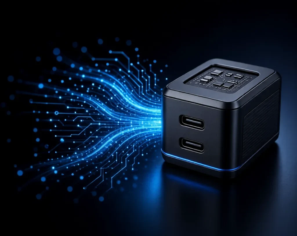
5 Powerful Advantages of GaN Technology
- Higher energy efficiency: less power lost as heat during conversion
- Greater power density: more power delivered from a smaller device
- Faster switching speeds: enables smaller passive components and compact designs
- Better thermal performance: runs cooler under sustained loads
- Strong reliability at high voltage: suited to demanding industrial and automotive use
Where GaN Technology Is Changing Technology
GaN has already moved from research labs into everyday products. It powers compact fast chargers for phones and laptops from major manufacturers. It is used in electric vehicle onboard chargers and inverters, where every gram and every watt of efficiency extends range. It is entering data center power supplies, where efficiency losses at scale translate into real electricity costs. It is also being explored in renewable energy inverters and 5G infrastructure, where high frequency, high efficiency switching is essential.
Real World Case Study: Dell’s Shift to GaN Charging
A documented example comes from Dell’s adoption of GaN based charging technology supplied by Navitas Semiconductor, reported by eeNews Europe. Dell’s adapter, manufactured by Chicony Power Technology, used GaNFast power integrated circuits for both its power factor correction and DC to DC conversion stages.
The original challenge was familiar: silicon based adapters for high power laptops were bulky and generated significant heat. Navitas’ design engineering and quality teams worked with Dell through rigorous performance and reliability testing before the adapter reached production.
The documented result was a smaller, more efficient charger built for a major global laptop brand, proof that GaN Technology could pass real world reliability standards at commercial scale, not just perform well in a lab. The lesson for readers: efficiency gains only matter when they survive rigorous engineering validation, and GaN has increasingly done exactly that.
The Hidden Challenges
GaN Technology is impressive, but it is not without friction. Manufacturing GaN chips is still more expensive than mature silicon processes, though costs are falling as production scales. Engineering teams also need experience to manage the very fast switching speeds correctly, since poor design can create electrical noise issues.
For extremely high power applications, like grid scale power conversion, silicon carbide, a related wide bandgap semiconductor, is often preferred instead. GaN is not a universal replacement for every kind of power electronics, it is the right tool for a specific and rapidly growing set of problems.
What Comes Next
Government backed research is accelerating GaN’s maturity. The U.S. Department of Energy’s PowerAmerica Institute continues funding wide bandgap semiconductor research to improve manufacturing and efficiency. Universities, including Arizona State University, are researching improved GaN doping processes to make devices more powerful and reliable.
As adoption grows across chargers, EVs, and data centers, expect GaN components to become cheaper, more common, and increasingly invisible, quietly doing their job inside devices you already own.
Frequently Asked Questions
Is GaN Technology safe to use in everyday chargers? Yes. GaN chargers from established manufacturers go through the same safety certifications as silicon based chargers, and their lower heat output can improve long term reliability.
Is GaN the same as silicon carbide? No. Both are wide bandgap semiconductors, but GaN tends to suit lower to mid power, high frequency applications like chargers and EV onboard systems, while silicon carbide often suits very high power applications.
Will GaN Technology fully replace silicon? Not entirely. Silicon remains cost effective for many applications. GaN is expanding fastest where efficiency, size, and high frequency switching matter most.
Is it worth buying a GaN charger? For anyone who travels or uses high power laptops and phones, a GaN charger’s smaller size and lower heat generation are genuine, practical benefits worth exploring.
Final Takeaway
GaN Technology is not a distant future concept. It is already charging phones, powering electric vehicles, and quietly improving data center efficiency today. As the semiconductor matures and costs continue to fall, it is set to become one of the defining materials behind the next generation of energy efficient technology.
The next time your charger feels surprisingly cool and impossibly small, there is a good chance gallium nitride is the reason why.