

What if the primary physical ceiling holding back clean energy is not the availability of sunlight, but the microscopic architecture of the panels collecting it?
For nearly seven decades, modern clean power has relied on crystalline silicon. Silicon is dependable, abundant, and proven. Yet beneath that familiar blue-black sheen lies a fundamental barrier known to physicists as the Shockley-Queisser limit. Single-junction silicon cells can theoretically capture only about 33% of incoming sunlight, while real-world commercial panels typically level off between 20% and 24%.
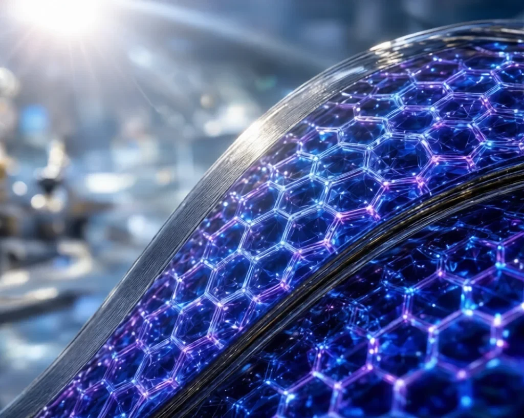
Enter perovskite solar cells. Over the past fifteen years, this synthetic class of materials has sprinted from a meager 3.8% laboratory efficiency in 2009 to certified tandem benchmarks exceeding 34% today. They promise lighter, cheaper, and radically more adaptable photovoltaics.
Yet alongside the breathless headlines comes a critical tension: laboratory records do not immediately translate to 25-year rooftop warranties. Below is an evidence-based look into the science, commercial breakthroughs, and engineering hurdles shaping the future of this photovoltaic frontier.
Table of Contents
How Perovskite Solar Cells Actually Work
The term “perovskite” does not refer to a single element. Instead, it describes any crystal structure sharing the general stoichiometry $ABX_3$, mirroring the atomic arrangement of calcium titanium oxide discovered in the Ural Mountains in 1839.
In photovoltaic research, scientists synthesize hybrid organic-inorganic halide perovskites. The crystal lattice typically combines:
- An organic or inorganic cation at site A (such as methylammonium, formamidinium, or cesium).
- A divalent metal cation at site B (predominantly lead or tin).
- A halide anion at site X (such as iodide, bromide, or chloride).
   [ A Cation ]  ---> Organic / Inorganic (Cs+, FA+, MA+)
        |
   [ B Metal ]   ---> Lead (Pb2+) or Tin (Sn2+)
        |
   [ X Halide ]  ---> Iodide, Bromide, Chloride
When sunlight hits this crystalline lattice, photons knock electrons free, creating electron-hole pairs (excitons). Because halide perovskites possess low exciton binding energy, these charges separate rapidly without wasting energy as heat.
Even more remarkable is their extraordinary light absorption coefficient. A perovskite layer just 500 nanometers thick absorbs as much visible light as a silicon wafer nearly 300 times thicker. Furthermore, by adjusting the ratio of halides (substituting iodide with bromide, for instance), chemists can tune the semiconductor bandgap between 1.2 eV and 2.3 eV, tailoring the material to absorb distinct bands of the solar spectrum.
Perovskite vs Silicon: A Side-by-Side Comparison
To evaluate whether perovskites can compete with or complement existing photovoltaics, we must contrast their baseline operational parameters.
| Performance Metric | Conventional Crystalline Silicon | Emerging Perovskite Solar Cells |
| Active Layer Thickness | 150 to 180 micrometers | 0.3 to 0.6 micrometers (thin film) |
| Material Synthesis Temp | High (1,400°C to 1,900°C for ingot purification) | Low (100°C to 150°C solution or vapor deposition) |
| Theoretical Single-Junction Limit | ~29.4% (practical Auger limit) | ~31% to 33% |
| Commercial Module Efficiency | 20% to 23% | 16% to 20% (pilot modules; higher in tandems) |
| Operational Lifespan | 25 to 30 years (degradation <0.5%/year) | 3 to 10 years (rapidly improving under testing) |
| Mechanical Profile | Rigid, brittle, heavy glass encapsulation | Flexible, lightweight, semi-transparent options |
The Tandem Solution: A Practical Evaluation Framework
Rather than pitting silicon against perovskite in a zero-sum contest, materials scientists frequently adopt a tandem approach.
When assessing the commercial viability of a next-generation photovoltaic technology, industry evaluators weigh three interlinked pillars: Levelized Cost of Electricity (LCOE), Process Integration, and Degradation Profiles.
                 [ COMMERCIAL VIABILITY ]
                           /  |  \
                          /   |   \
                         v    v    v
        [ LCOE ]        [ Integration ]        [ Durability ]
     (Capex + Yield)   (Silicon lines)      (IEC 61215 tests)
- LCOE Impact: Efficiency gains must outpace additional layer manufacturing costs. Adding a few percentage points of cell efficiency reduces total balance-of-system expenses (land, wiring, steel framing, installation labor) per installed megawatt.
- Process Integration: Can factories drop the new technology into existing manufacturing chains? Monolithic perovskite-silicon tandem cells coat a wide-bandgap perovskite layer directly atop a standard silicon bottom cell. The top layer absorbs high-energy blue and green photons, while the underlying silicon absorbs lower-energy red and near-infrared photons.
- Durability and Warranties: Bankable solar installations require modules that resist moisture, oxygen, heat cycling, and ultraviolet radiation under standard international protocols.
Real-World Progress: From Cleanrooms to Commercial Arrays
The transition from academic curiosity to working technology is already well underway. In Europe and Asia, specialized photovoltaic manufacturers have established multi-megawatt pilot lines producing full-sized commercial tandem modules.
Companies like Oxford PV, LONGi, and Hanwha Qcells have moved beyond coin-sized lab samples to produce full-scale commercial panels. In pilot installations across utility testing grounds, perovskite-on-silicon panels are operating in outdoor field conditions alongside traditional panels to measure real-world performance under variable cloud cover, humidity, and thermal cycling. Early field data shows that tandem systems produce disproportionately higher energy yields during dawn, dusk, and overcast conditions, thanks to the wide spectral absorption profile of the engineered top cell.
Verified Data: Decoding the Efficiency Records
When reading about solar records, context is everything. Independent testing bodies like the National Renewable Energy Laboratory (NREL) rigorously verify device metrics to separate verified breakthroughs from marketing claims.
According to the official NREL Best Research-Cell Efficiency Chart:
- Single-junction perovskite laboratory cells hold certified records exceeding 26.5%, rivaling the best monocrystalline silicon research cells.
- Perovskite-silicon tandem research cells have officially reached certified efficiencies of 34% to 35% on small-area research devices (1 cm² or smaller).
Distinguishing Lab Cells from Field Modules:
A tiny 1 cm² research cell tested inside a temperature-controlled glovebox at 25°C does not perform identically to a two-square-meter module exposed to desert heat and summer storms. When cells are wired into larger modules, resistance losses and edge effects typically shave several percentage points off the headline efficiency figure. Commercial tandem modules currently target initial nameplate ratings of 25% to 29%, which remains a notable step up from standard 22% silicon arrays.
Practical Applications Beyond Rooftops
Because perovskite thin films can be printed from liquid inks onto flexible substrates at modest temperatures, they unlock applications previously unsuited for heavy silicon slabs:
- Building-Integrated Photovoltaics (BIPV): Semi-transparent perovskite coatings can be laminated directly inside architectural glass and curtain walls, transforming office building windows into power-generating surfaces.
- Agrivoltaics: Tailored chemical compositions allow specific photosynthetic wavelengths of red and blue light to pass through to crops below while harvesting unused spectrum bands for electricity.
- Wearable and Internet-of-Things (IoT) Devices: High performance under indoor ambient lighting (fluorescent and LED) enables indoor sensors, smart packaging, and asset tags to operate battery-free.
- Aerospace and Drones: Exceptional power-to-weight ratios make flexible thin films attractive for stratospheric drones, satellites, and portable field gear where every gram counts.
Technical Challenges: Stability, Cost, and Lead Toxicity
Despite their rapid ascent, perovskite solar cells face genuine material hurdles that prevent instantaneous market dominance.
1. Environmental Stability and Degradation
Halide perovskites are chemically sensitive to moisture, oxygen, ultraviolet light, and heat. Water molecules dissolve methylammonium salts, triggering a phase breakdown into inactive compounds. Furthermore, under sustained illumination and thermal stress above 60°C, ion migration inside the crystal lattice can degrade contact interfaces and reduce output.
2. Commercial Encapsulation Costs
To keep perovskites stable for decades, manufacturers cannot rely on ordinary polymer backsheets. They must develop hermetic sealants, atomic layer barrier coatings, and inert gas seals. If encapsulation costs become too high, the economic advantage of solution printing disappears.
3. The Lead Dilemma
The highest-performing perovskites rely on water-soluble lead halides. While the total volume of lead in a panel is minimal (fractions of a gram per square meter), the environmental hazard stems from potential rainwater leaching if a glass panel cracks during hail storms or fire.
Researchers are investigating two parallel paths: developing stable, lead-free alternatives based on tin ($Sn$) or bismuth ($Bi$), and engineering specialized cross-linked polymer wraps that chemically bind and sequester lead within the panel even if the outer glass shatters.
Common Misconceptions vs The Scientific Reality
The Misconception: “Perovskite solar cells are designed to replace silicon completely within the next couple of years.”
The Reality: The solar industry has invested hundreds of billions of dollars into high-throughput silicon wafer manufacturing, supply chains, and automated assembly plants. Scrapping that infrastructure is neither feasible nor financially sound.
Instead of replacing silicon, perovskite acts as a performance multiplier. The near-term commercial strategy is almost universally tandem deployment: coating perovskite layers atop existing silicon production lines to boost module output without overhauling balance-of-system architecture.
What Engineers, Investors, and Readers Should Do Next
Whether you follow clean technology from an investment, engineering, or policy perspective, watching the right milestones will help you cut through the hype:
- Watch Accelerated Stress Standards: Track whether emerging modules achieve formal certification under the IEC 61215 standard, which subjects panels to damp heat (85°C at 85% relative humidity for 1,000+ hours), mechanical stress, and thermal cycling.
- Scrutinize Area Measurements: When evaluating new performance claims, verify the active device area. A result verified on an aperture area above 200 cm² indicates genuine pilot manufacturing progress, whereas a result on 0.1 cm² remains an early-stage lab proof of concept.
- Follow Primary Research Outlets: Rely directly on peer-reviewed updates from the U.S. Department of Energy Solar Energy Technologies Office and the annual progress summaries published in journals like Nature Energy and Joule.
Frequently Asked Questions
What makes perovskite solar cells unique compared to older thin films?
Unlike earlier thin films such as cadmium telluride (CdTe) or CIGS, perovskites boast unusually high defect tolerance. They can achieve high charge carrier mobility and long diffusion lengths even when synthesized rapidly at low temperatures from liquid solutions, avoiding expensive vacuum chambers.
Can perovskite solar cells function in rainy or humid climates?
Early unsealed prototypes degraded within hours of humidity exposure. However, modern commercial prototypes incorporate impermeable multi-layer barrier films and advanced edge sealants that shield the active perovskite layer from moisture intrusion during outdoor operation.
Are lead-free perovskite solar cells viable today?
Tin-based ($Sn$) perovskites are the most widely studied lead-free alternative, but divalent tin oxidizes rapidly when exposed to air ($Sn^{2+}$ to $Sn^{4+}$), reducing device efficiency and stability. Lead-free formulations remain an active area of foundational research and have not yet matched the performance of lead-halide cells.
How much could perovskite tandems lower household power bills?
Because tandem panels generate roughly 20% to 30% more wattage within the exact same surface footprint, installation, mounting hardware, and roof space requirements decrease per unit of energy generated. Over time, this efficiency boost can lower the overall balance-of-system cost for residential and commercial rooftop solar.
When will perovskite solar panels be widely available for home installation?
Pilot modules are undergoing utility field tests and small-scale commercial deployments today. Widespread availability for standard residential installations is projected to expand gradually over the next three to six years as manufacturers scale volume manufacturing and validate 20-year durability claims.
The progression of perovskite photovoltaics illustrates how materials science can transform a clean-energy landscape once constrained by physical limits. While long-term durability and encapsulation hurdles remain under intense development, pairing perovskite crystals with established silicon substrates offers a practical path toward cleaner, more efficient, and more versatile solar power.