
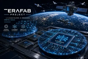
Every major technology revolution eventually slams into a physical wall. Software developers write brilliant artificial intelligence algorithms, but those models cannot think without silicon. Autonomous robot fleets cannot navigate streets without edge processors. Space exploration constellations cannot route signals without compute nodes hardened against cosmic radiation.
For the past two years, the tech sector operated under a single brutal reality: the world’s most powerful AI systems were constrained by a tiny handful of semiconductor cleanrooms scattered across Taiwan, South Korea, and the United States. Global demand for advanced silicon outstripped supply, lead times stretched into quarters, and geopolitical friction turned semiconductor fabrication into the ultimate strategic bottleneck.
Now imagine a countermove born out of pure frustration with that bottleneck. What happens when the race for AI shifts from training larger models to building the machines that build AI?
Enter Terafab, Elon Musk’s audacious effort to bypass traditional semiconductor supply chains by creating a vertically integrated chipmaking empire.
Table of Contents
1. What Is Terafab?
At its foundation, Terafab is a planned mega-scale semiconductor fabrication venture designed to consolidate every link of the microchip manufacturing chain under a single operating structure.
In modern electronics, making a processor is splintered across multiple continents. One company writes the architectural blueprint. Another company prints microscopic circuits onto raw silicon wafers. A third firm manufactures high-bandwidth memory chips. Finally, an outsourced assembly and test facility packages those delicate dies into a finished chip.
Terafab proposes ending that fractured model. The initiative, organized as a joint venture involving Tesla, SpaceX, and xAI, with reported framework discussions alongside established semiconductor giants like Intel, aims to house silicon wafer fabrication, memory integration, advanced packaging, and rigorous testing within a unified complex in Texas. Its stated mission is straightforward: churn out high-volume, highly specialized computing hardware engineered directly for physical AI, robotics, and aerospace infrastructure.
2. Why Elon Musk Wants It
Musk’s industrial strategy has always followed a predictable playbook: when an external supplier becomes an existential choke point, bring the capability in-house. Tesla did it with battery cells and structural castings. SpaceX did it with rocket engines and avionics.
Today, the choke point is silicon.
Musk publicly projected that the combined compute demands of Tesla’s self-driving Cybercabs, Optimus humanoid robots, and SpaceX’s orbital communication networks will exceed the entire world’s current chipmaking output. While company statements emphasize continued appreciation for existing partners like TSMC and Nvidia, corporate announcements from SpaceX and Tesla frame the gulf between global chip output and their future compute targets as unsustainable.
It is essential to separate documented company actions from Musk’s long-term projections. Officially confirmed filings and public announcements in 2026 outline an initial Texas investment phase pegged at roughly $16.8 billion, with county filings referencing multi-phase expansions scaling past $100 billion over time. However, claims that Terafab will deliver upwards of one terawatt of annual compute output represent future ambition rather than operational reality.
3. The Bigger Idea Behind Terafab
Terafab is not envisioned as a general-purpose commercial foundry that bids on contracts to build laptop CPUs or smartphone chips. It is an internal engine designed for full vertical integration.
The conceptual architecture combines several distinct layers:
- Custom Logic Fabrication: Tailoring silicon logic directly to neural network weights, stripping out unnecessary legacy PC instructions to maximize power efficiency.
- On-Site Advanced Packaging: Connecting compute dies and high-bandwidth memory side-by-side on microscopic silicon interposers, eliminating months of international shipping between distinct fab and packaging contractors.
- Extreme Environment Hardening: Fabricating radiation-tolerant processors engineered to operate in the vacuum and intense cosmic ray bombardment of low Earth orbit, supporting SpaceX’s long-range ambitions for space-based satellite compute clusters.
4. Comparing Traditional Fabs with Terafab
To understand why this project causes both awe and skepticism across the semiconductor industry, we must contrast it with traditional manufacturing.
| Dimension | Traditional Semiconductor Model (e.g., TSMC, Samsung) | The Terafab Concept |
| Business Structure | Pure-play foundry serving hundreds of global customers | Dedicated captive/partner fab serving internal ecosystem needs |
| Integration | Geographically fragmented across design, fab, and OSAT packaging | Consolidated: design, wafer fab, memory, packaging under one roof |
| Iteration Cycle | Months between tape-out, external fab queuing, and delivery | Rapid prototyping and direct feedback loops into hardware products |
| Capital Architecture | Financed through broad customer demand and diverse markets | Dependent on deep corporate balance sheets and targeted internal demand |
| Supply Chain Exposure | High global exposure; vulnerable to geopolitical sea lanes | Centered domestically, but still dependent on imported tools (e.g., ASML lithography) |
| Operational Risk | Shared risk distributed across diverse commercial clients | Concentrated risk tied directly to Tesla, SpaceX, and xAI execution |
Neither approach is an absolute winner. The traditional model offers immense scale, shared research costs, and stability across varied customer cycles. Terafab trades that risk-pooling for custom speed, tighter hardware-software cohesion, and strategic independence.
5. An Illustrative Path: From Sand to Robot
To see the practical intent behind this model, consider how a next-generation robotics processor might theoretically move through such a facility.
Note: This is an illustrative workflow demonstrating the engineering concept, not a log of an active production run.
- Design Simulation: Neural network researchers design an accelerator specifically tailored to balance motor control, vision processing, and sensor fusion for a humanoid robot.
- Wafer Stepping: Instead of shipping design files across an ocean, the blueprint is transferred directly to on-site cleanrooms where photolithography scanners expose circuit patterns onto silicon wafers.
- Co-Packaged Memory: The silicon die is sliced and placed directly next to custom memory dies using high-density interconnects, bypassing traditional packaging plants in Southeast Asia.
- Stress Testing and Deployment: The completed unit is baked in thermal chambers, tested against vibration, and driven down the highway to an assembly line where it is bolted directly into a robot torso.
By compressing that physical journey from thousands of miles down to a single site, development cycles that normally consume eighteen months could theoretically occur in a fraction of that time.
6. Expert Interpretation: Ambition Meets Silicon Reality
Independent semiconductor analysts view the project with a blend of respect and extreme caution.
On an engineering level, bringing fab, memory, and packaging into closer physical proximity is a sensible architectural evolution. High-bandwidth interconnects and thermal management are the primary bottlenecks of AI acceleration today. If a facility could streamline those transitions, the latency gains would be genuine.
However, execution is extraordinarily difficult. Making advanced chips is widely considered the most complex manufacturing endeavor in human history:
- Yield Curves: A new fab does not simply turn on and produce flawless wafers. It takes years of microscopic chemical tuning to bring wafer defect rates down to commercially viable levels.
- Tool Access: No company builds a fab from scratch without specialized supplier equipment. Advanced extreme ultraviolet (EUV) lithography systems come from ASML in the Netherlands, while critical deposition and etch equipment relies on suppliers like Applied Materials, Lam Research, and Tokyo Electron. Capital alone cannot speed up the multi-year manufacturing backlog for these precision machines.
- Specialized Talent: Operating a commercial fab requires thousands of deeply specialized physicists, chemical engineers, and process technicians. Texas possesses a growing semiconductor corridor, but staffing a facility of this magnitude poses an immense hiring hurdle.
7. Interpreting the Numbers
Public numbers surrounding mega-projects often blur into incomprehensible abstraction. Let us put the publicly discussed figures into practical perspective:
- The $16.8 Billion Initial Phase: Tesla and SpaceX committed an initial phase investment of roughly $16.8 billion. For context, building a single cutting-edge leading-edge fab module today routinely costs between $15 billion and $20 billion. This indicates that initial funds are tailored to establish a functional, high-end pilot and initial manufacturing footprint rather than an instantaneous global supply network.
- The “One Terawatt” Compute Claim: Company announcements cited a combined internal demand exceeding one terawatt of compute. In electrical engineering terms, one terawatt is one trillion watts, roughly equivalent to the total instantaneous electrical generation capacity of the entire United States power grid. Using power capacity as a metric for compute underscores that future AI constraints will be dictated as much by energy access as by wafer counts.
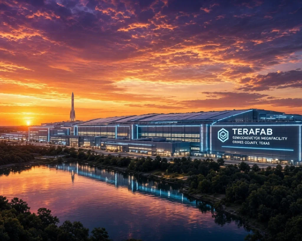
- Facility Footprint Projections: Local Texas development filings and company renders describe a footprint spanning millions of square feet. If completed across all proposed phases, it would dwarf existing industrial landmarks, reflecting an unprecedented physical consolidation of semiconductor tooling.
8. Strategic Advantages and Clear Limitations
Every industrial bet comes with distinct trade-offs.
Potential Strategic Advantages
- Complete Hardware-Software Co-Design: Chips can be customized for exact neural network operations, eliminating silicon overhead.
- Shielding from Geopolitical Supply Shocks: Shielding core vehicle and aerospace production from overseas shipping disruptions or regional blockades.
- Compressing Iteration Speed: Slashing the turnaround time between architectural design revisions and physical silicon testing.
Real Technical Limitations
- Immense Capital Drain: Semiconductor plants demand billions in recurring capital expenditures simply to stay current with shrinking process nodes.
- Extreme Yield Vulnerability: Low initial yields can result in billions of dollars in scrapped silicon wafers before reaching stability.
- Intense Energy Requirements: Operating massive cleanrooms and advanced lithography tools requires steady, uninterrupted baseload power, creating heavy demands on regional energy infrastructure.
9. The Common Misconception
A widespread misconception surrounding Terafab is that building an enormous semiconductor building guarantees instant, unlimited AI computing power.
It does not. Silicon manufacturing is merely one link in a fragile computing ecosystem. Having finished chips is meaningless without adequate high-bandwidth memory supply, dependable electrical grids to power training clusters, advanced liquid-cooling systems to dissipate megawatts of heat, and mature compiler software to orchestrate model parallelization.
A chip factory produces parts; an AI infrastructure requires a coordinated symphony of energy, thermal engineering, and software optimization.
10. Real-World Applications: What It Means for Ordinary People
Why should an everyday technology user care whether an automaker or aerospace company manufactures its own silicon?
The ripple effects touch everyday life:
- Everyday Autonomous Safety: If custom edge processors can be produced in high volume at lower unit costs, advanced active safety and driver-assistance features can expand across mass-market vehicles rather than remaining luxury add-ons.
- Robotics in Daily Logistics: The deployment of assistive humanoid robots in warehouses, factories, and eventually eldercare hinges on cost-effective, low-latency computing hardware that can react to dynamic environments in real time.
- Resilient Consumer Cloud Services: Broadening domestic manufacturing relieves supply pressure across commercial data centers, helping prevent artificial intelligence services and business cloud tools from facing severe capacity rationing.
11. Practical Framework: How to Evaluate Megaprojects
Whenever a visionary technologist announces a project that sounds like science fiction, use this systematic eight-step evaluation lens:
$$\text{Vision} \longrightarrow \text{Technology} \longrightarrow \text{Infrastructure} \longrightarrow \text{Capital} \longrightarrow \text{Manufacturing} \longrightarrow \text{Scalability} \longrightarrow \text{Economics} \longrightarrow \text{Real-World Impact}$$
- Vision: What fundamental physical problem does the project claim to solve?
- Technology: Does the underlying physics and chemistry exist today, or does it require unproven breakthroughs?
- Infrastructure: Are the required baseload power, water recycling, and regional supply lines available?
- Capital: Is funding secured through committed operational cash flows, or dependent on speculative market conditions?
- Manufacturing: Can the project achieve acceptable defect rates and high yields at scale?
- Scalability: Can production expand without depleting scarce global resources or critical equipment backlogs?
- Economics: Does the manufactured component cost less per unit of performance than buying from established open foundries?
- Real-World Impact: Does the output meaningfully improve end-user products, or does it remain an internal showcase?
Applying this framework to Terafab shows a compelling vision backed by initial committed capital, but one that faces monumental hurdles across infrastructure, tooling access, and manufacturing yields.
12. Tracking What Comes Next
For technology observers, investors, and engineers following the evolution of Terafab, the path forward requires tuning out sensational headlines and focusing on verifiable physical milestones:
- Monitor Regulatory and Environmental Permits: Look for air quality, water utilization, and power grid interconnect approvals filed with Texas state authorities.
- Watch Tool Delivery Schedules: Track disclosures regarding lithography and cleanroom equipment deliveries from critical global suppliers.
- Inspect Corporate SEC Filings: Follow official quarterly 10-Q and 10-K filings from Tesla to track actual capital expenditure allocations versus planned projections.
- Look for Verified Silicon Tape-Outs: Wait for independently benchmarked hardware announcements (such as verified production runs of Tesla’s next-generation AI processors) rather than pilot renders.
The semiconductor industry is unforgiving to hype. Whether Terafab emerges as a historic manufacturing milestone or a sobering lesson in the extreme difficulty of chipmaking will not be decided by stage presentations, but by the relentless physics of the cleanroom floor.